The observation of chemical mechanical polished film by 2- dimension elliposmeter
As device dimensions continue to shrink to half micron and smaller ,planarization by chemical mechanical polishing ( CMP ) technique shifts from an optional processing method to a critical enabling technology for DRAMs as well as microprocessors and ASICs. For the next-generation semiconductor device fabrication, the number of CMP steps required for a single device can be greater than ten. One of main CMP applications for multi-level interconnect technology is to planarize and smooth the interlayer dielectric film. Currently it is believed that it may not be sufficient to only control the film thickness after the CMP process. In addition, it is required to assure the intrinsic properties of the remained film such as film defect level, film density, etc. In order to maintain the thin film with high quality, it is very critical to understand and CMP process accurately. The precise control involves in the development of thin film metrology tool which can sample a large amount of measurement data with excellent statistical metrology software support. Heureka Co., Ltd. Has developed ellipsometer of two dimensional measurement type, by which throughput and the data measurement speed can increase by a factor of several hundred thousand times over a conventional one point measurement type ellipsometer. In addition, Heureka's two dimensional type ellipsometer has also shown the ability of simultaneous measurement of film thickness and refractive index of oxide film after certain CMP process described below:
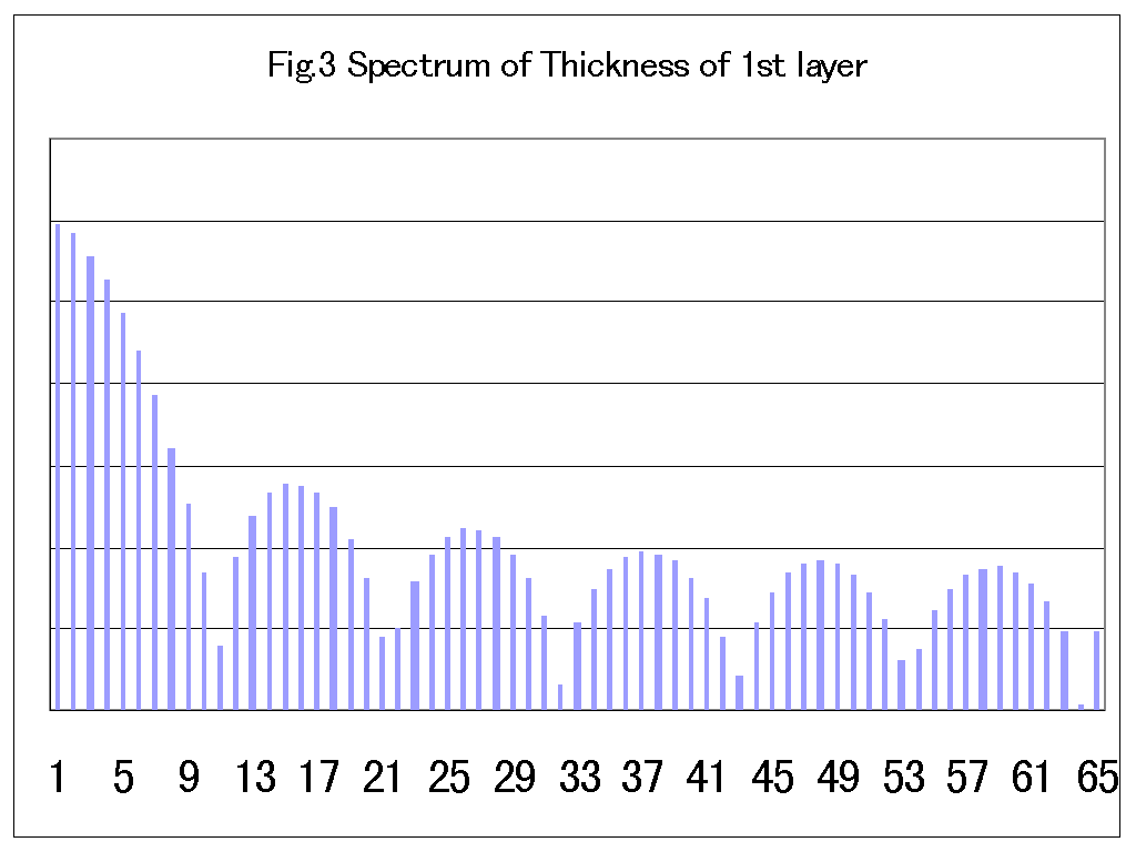
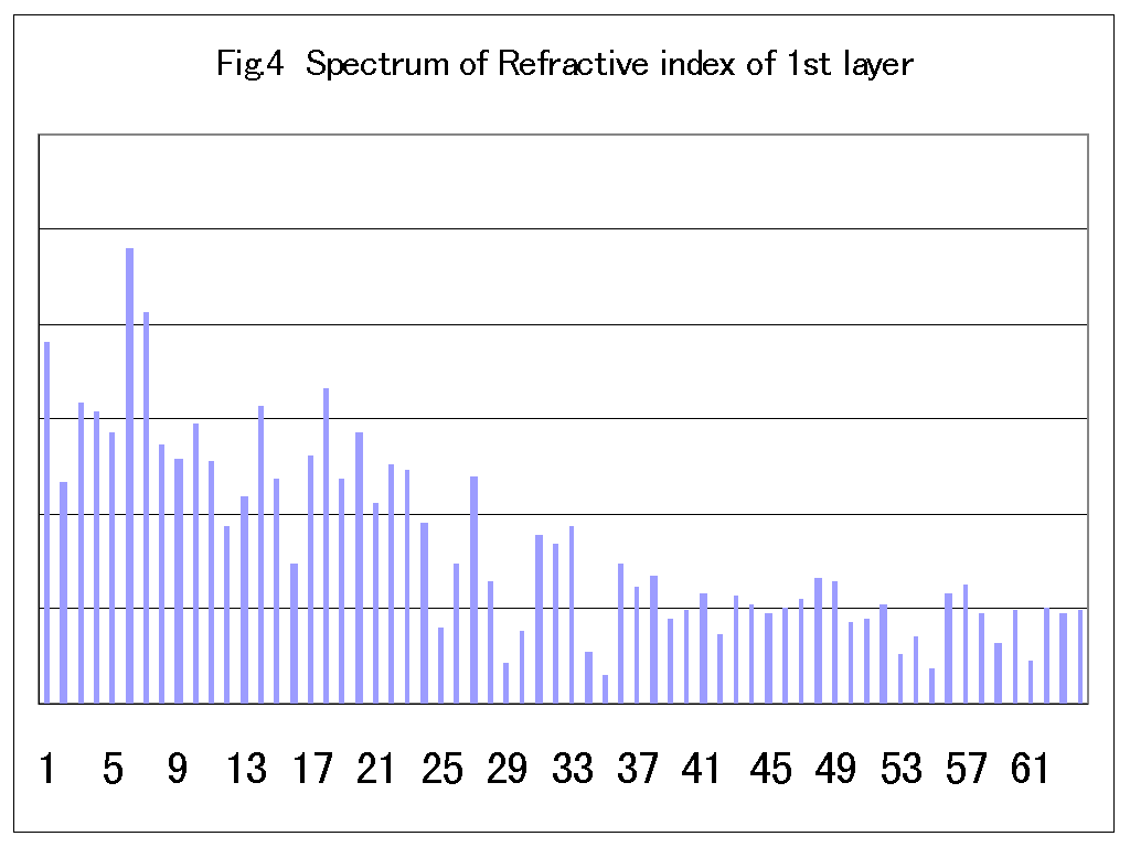
Figures 1 and 2 display the film thickness and the refractive index, measured at 127,000 points, of PETEOS film deposited on 150ćoāė Si wafer, which was polished with a CMP machine ( from the original 1.5 micron to the final film thickness of about 0.8 micron ). Figure 3 is a spectrum by Fourier transform of typical film thickness and refractive index. The repetitive patterns seen in film thickness ( shown in Fig. 1 ) are expressed as the periodic peaks of the spectrum ( Fig. 3). The characteristic of refractive index spectrum shows not only some periodic peaks but also irregular and discontinuous peaks. This characteristic is influenced by the extent of CMP-induced defects in the remained film. We believe this distinctive characteristic of refractive index can be potentially useful barometer for determining the intrinsic film quality.
ü@ü@ü@ü@ü@ü@ü@ü@ü@ü@éeéēéćüDéPü@ü@ü@ü@ü@ü@ü@ü@ü@ü@ü@ü@ü@ü@ü@ü@ü@ü@ü@ü@ü@ü@ü@ü@ü@ü@ü@ü@ü@ü@éeéēéćüDéQ
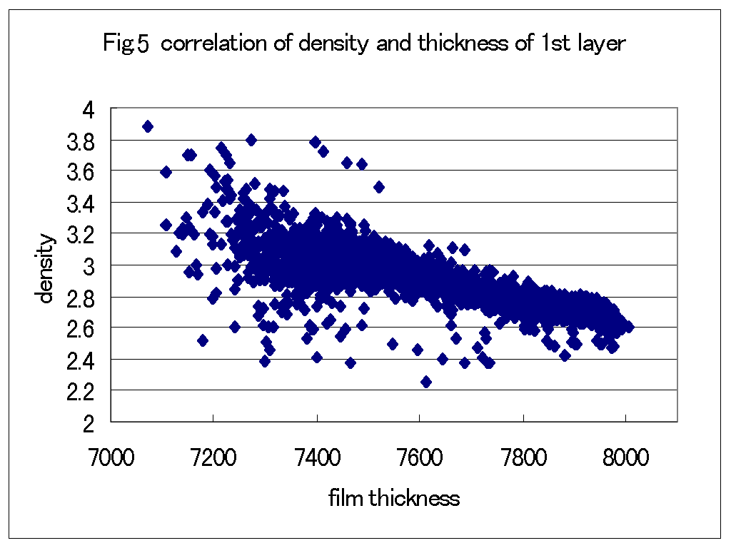
Returning to Figs. 1 and 2, we notice that there is a definite correlation between film thickness and refractive index of the PETEOS film. Our data clearly show that thinner film thickness region exhibits higher refractive index while the thicker film thickness region has lower refractive index. The density of this film can be calculated from the refractive index by the Lorenz-Lorenz equation. figure 5 is a scatter plot of the density and the film thickness of this sample. This figure again clearly shows a strong linear negative correlation between these two parameters. This linear negative correlation is quite surprising because the refractive index and the film thickness are independent parameters originally. No recognizable correlation between these two parameters have ever reported before ( for example, such a correlation has never been observed experimentally in the case of thermally grown oxide film. ).
The real causes for this unexpected correlation has not been determined. One plausible interpretation to this phenomenon is based upon the idea that the polishing pressure in actual polishing condition was not constant throughout the surface of the sample. Generally, the polishing rate is directly proportional to the polishing pressure ( Preston Equation ). Therefore, if higher pressure is locally applied to certain location in the sample surface, not only the film thickness of that higher pressure region becomes thinner but also maybe denser due to the higher impact towards PETEOS, which certainly has more open structure than thermally grown oxide film.
In conclusion, we show that Heureka's new two dimensional type ellipsometer with the capability of faster sampling rate and analysis of larger amount of data offers a new evaluation technique for the thin film processing in semiconductor industry.